December 13, 2022
Toray Engineering Co., Ltd.
Commence Sales of INSPECTRA® CR-III, Semiconductor Chip Inspection System with the Industry's Highest Level of Accuracy
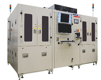
INSPECTRA® CR-Ⅲ
TASMIT Inc. (TASMIT, Head office: Kohoku-ku, Yokohama, Kanagawa, CEO: Kenji Sato, hereinafter "TASMIT") has developed the INSPECTRA® CR-III, semiconductor chip inspection system with the industry's highest level of accuracy. Sales will commence in January 2023.
This system was realized by combining the highly accurate inspection function of the INSPECTRA® SR-III semiconductor wafer inspection system with highly efficient chip handling technology. It is the first dedicated semiconductor chip inspection system in the industry. It is characterized by being approximately five times more accurate than conventional systems that have been used in the past, while having almost the same efficiency as conventional products.
TASMIT will propose the INSPECTRA® CR-III to customers who are developing power semiconductors for automotive applications, where the need for highly precise and efficient semiconductor chip inspection in particular is increasing. It aims to achieve orders amounting to 600 million yen in FY2023 and 1 billion yen in FY2025.
As utilization scenarios for electricity expand toward the realization of a decarbonized society, power semiconductors that control large voltages and currents are gaining attention. In automotive applications in particular, minimizing electricity loss and reducing vehicle size and weight directly affect performance, such as extending cruising range. Thus, further performance improvement of power semiconductors is expected toward the expansion of electric vehicles.
Currently, the performance of power semiconductors is improving as a result of circuit miniaturization and multilayering, as well as chip miniaturization. In the conventional power semiconductor manufacturing process, final semiconductor chip inspections have traditionally used electronic component inspection systems. However, in automotive applications that use large amounts of electricity, small defects in power semiconductors can lead to major problems. Recently, the need has been growing for more precise semiconductor chip inspection to further improve safety and reliability.
In response to this need, TASMIT has applied its high-precision optical microscope technology cultivated through its semiconductor wafer inspection systems to chip inspection applications. This has made it possible to detect defects up to the 1 micrometer class, which is approximately five times more accurate than the equipment conventionally used for semiconductor chip inspection. Furthermore, TASMIT has succeeded in maintaining inspection efficiency at the same level as conventionally used equipment by developing a mechanism that simultaneously transfers and inspects multiple semiconductors using the highly efficient semiconductor chip handling technology that Toray Engineering has developed in its semiconductor packaging equipment business.
Furthermore, this model can be combined with "AI-ADC" (Automatic Defect Classification), which, like other models in the INSPECTRA® series, has both an efficient AI-based learning and defect classification functions, further increasing inspection efficiency.
This system will be exhibited in a panel display at the SEMICON Japan exhibition, which will be held at Tokyo Big Sight from December 14, 2022.
TASMIT will contribute to the improvement of semiconductor performance and reliability through the deployment of various optical and electron beam-type semiconductor inspection systems. It will also contribute to the realization of a low-carbon society by expanding utilization scenarios for electricity.
Toray Engineering provides solutions for solving all kinds of issues in manufacturing by using its technologies, engineering, and know-how.
Note
| 1. Product name | : | INSPECTRA® CR-Ⅲ |
| 2. Product features | : | ・Semiconductor chip inspection system with the industry’s highest level of accuracy ・High inspection efficiency through highly efficient semiconductor chip handling technology ・High efficiency through combination with AI-ADC system |
| 3. Usage | : | Inspection of power semicondcutors |
| 4. Order goals | : | 600 million yen in FY2023 1 billion yen in FY2025 |
<Reference>
About “SEMICON Japan” Exhibition
| 1. Exhibition name | : | SEMICON Japan 2022 |
| 2. Venue | : | Tokyo Big Sight |
| 3. Date | : | December 14--16, 10:00--17:00 |
| 4. Booth no. | : | 4016 |