Introducing Electron Beam Semiconductor Wafer Pattern Verification System NGR®5500 with the Highest Level of Throughput and Accuracy in the World for Semiconductor Circuit Inspection
Mar. 3, 2022
Toray Engineering Co., Ltd. (Head office: Chuo-ku, Tokyo, CEO & COO: Takashi Iwade, hereinafter ‟Toray Engineering”) announced that its subsidiary TASMIT, Inc. (Head office: Yokohama, Kanagawa, CEO: Kenji Sato, hereinafter ‟TASMIT”) has developed the electron beam semiconductor wafer pattern verification system NGR®5500 with the highest level of throughput and accuracy in the world for semiconductor circuit inspection. Sales of the system will commence in April 2022.
NAND flash memory is moving toward multiple layers for higher performance, and there is further shrink of DRAM memory and logic semiconductors. This system will be offered to manufacturers of these semiconductors to contribute toward improving the efficiency of their manufacturing processes. The sales target is 5 billion JPY in FY 2022 and 7 billion JPY in FY 2025.
The NGR®series of electron beam semiconductor wafer pattern verification systems comprises systems that use electron microscope images to measure the differences between the designed patterns of circuits with those actually transferred in the semiconductor manufacturing process. Using Toray’s unique system design technology, images having a wide field of view with small distortion can be obtained, allowing high-precision inspection to be carried out with speed and enabling adjustments to be made early in the process. This can achieve improved manufacturing efficiency, for which the system is highly recognized.
Toward improving the performance of semiconductor devices, layered circuits are increasing in the number of layers and circuits are becoming more shrink . Memory holes and trenches for connecting circuits between layers are becoming deeper with the increase in the number of layers, resulting in demand for inspection systems that can carry out shape inspection of the bottoms of these holes and trenches with high accuracy. Furthermore, to improve the positioning accuracy of shrink circuits, it is required to carry out inspections at the nanometer level with high efficiency. Currently, there are inspection systems offered for mainstream semiconductor devices with 96 to 128 layers. However, there are few systems that can conduct a wide range of accurate and fast inspections for high-performance NAND flash memory semiconductors—which are being considered for development and mass production with 150 and more layers toward even higher performance—and for DRAM memory and logic semiconductors which are becoming even more miniaturized.
To address this issue, TASMIT used its unique electron beam control, lens electrode optimization, ultrahigh vacuum, and high voltage technologies and succeeded in being the first in the world to raise the acceleration voltage of electrons used in electron beam microscopes for semiconductor inspections up to 50 kV. Raising the acceleration voltage allows images with high resolutions to be obtained. This enables inspections of NAND flash memory semiconductors with 150 and more layers—currently being developed—and circuits that are several nanometers wide to be conducted with high accuracy. At the same time, high-speed inspection using the NGR®series’ feature of being able to obtain images having a wide field of view with low distortion is also achieved.
The Toray Engineering Group will continue to contribute to society through the pursuit of cutting-edge inspection technology and proposals of solutions that make full use of our technology, engineering technology, and know-how.
The details of the NGR®5500 being launched are as follows.
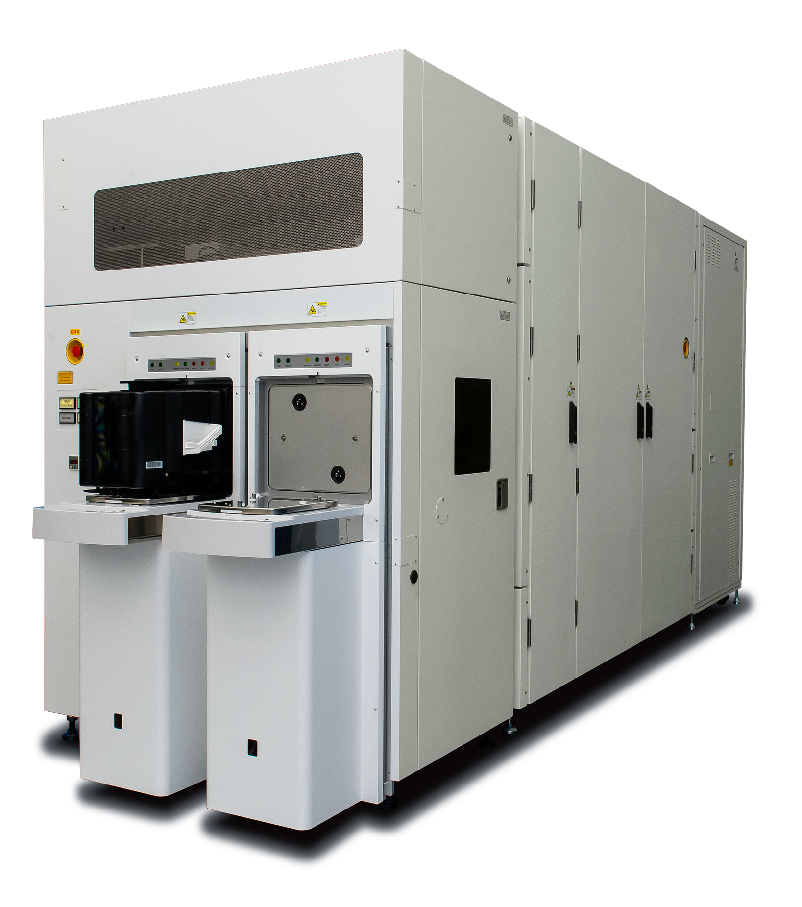
Product name
NGR®5500
Product features
- High-speed inspection by acquiring images having a wide field of view with low distortion
- Die to Database application that conducts inspection and measurement through high-accuracy comparison of acquired images with design data
- Inspection and measurement of overlays and high aspect ratio (HAR) structural patterns using transmission images obtained from the world’s highest class of high-acceleration electron beam microscope
Usage
- OPC*1 optimization and hot spot*2 detection during developmental stage
- Hot spot monitoring in mass production lines
Sales goals
- 5 billion JPY in FY 2022
- 7 billion JPY in FY 2025
- Optical proximity correction
This is a technology that controls the deformation of transfer patterns due to optical proximity effect—which occurs easily with the miniaturization of circuit patterns—by calculating in advance the occurrence of such deformations and compensating for them. - Hot Spot
Locations where defects occur easily.
Reference
TASMIT, Inc.
| Head office | Yokohama, Kanagawa |
|---|---|
| Established | July 2000 |
| Capital | 100 million JPY |
| Representative | CEO Kenji Sato |
| Line of business | Development, manufacturing, and sales of inspection equipment for semiconductors |
以上