Bonding Technology Developed for Ultra-Thin Semiconductors to Deliver Industry’s Highest-Level Throughput
―To Support Mass Production of Advanced Semiconductors and Next-Generation Photonic Integrated Circuits―
October 6, 2025
Toray Engineering Co., Ltd.
In the “Research and Development Project of the Enhanced Infrastructures for Post-5G Information and Communication Systems” (hereinafter “the project”) subsidized by NEDO, Toray Engineering Co., Ltd. has developed a bonding technology (hereinafter “the technology) for ultra-thin semiconductors to deliver industry-leading high throughput for mass production of advanced semiconductors and next-generation photonic integrated circuits to be used in post-5G information and communication systems.
The technology is based on laser transfer technology used for applications such as bonding microLEDs (Light Emitting Diodes) to display substrates. It enables the production of less than 20 µm semiconductor chips used for advanced semiconductors or compound semiconductor chips with a thickness of less than 1 µm used for next-generation photonic integrated circuits to be produced with a tenfold greater efficiency than before while maintaining the accuracy required for mass production.
1. Background
For advanced semiconductors required for post-5G information and communication systems, thinner semiconductor chips are increasingly required for higher performance and lower power consumption. Semiconductor chips with a thickness of 20 µm or less present the issue of drastically reduced yields during handling, making it important to develop technology that can maintain yields while achieving the throughput required in mass production.
In particular, there is growing demand for high-throughput bonding technology for ultra-thin chips in fields such as 3D packaging technology, which has high expectations as a manufacturing technology for advanced semiconductors, and next-generation photonic integrated circuits supporting post-5G communication technology.
2. Results
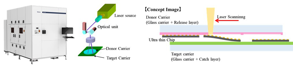
(1) Development of a laser transfer technology
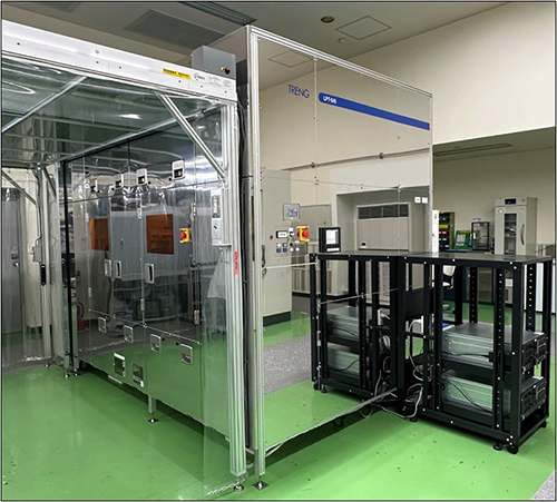
Toray Engineering has developed in the project*1 a high-accuracy laser processing position control technology and a laser photonic system optimized for the laser transfer process. By combining these technologies, we have developed a scan system that peels ultra-thin chips from donor carrier and transfers them to target carrier with high yields by irradiating the chip with a small laser starting with the edge of the chip. The system has allowed the posture of chips to be stabilized while being peeled by taking advantage of the company’s proprietary laser processing technology to optimize the scanning patterns of the laser. As a result, we have achieved a bonding technology with the transfer position accuracy, yield, and throughput at an industry’s highest level*2. In addition, the equipment developed in the project supports 300 mm wafers and the 515 mm x 500 mm panel size mainly used in the production lines of advanced semiconductors, allowing for the evaluation of ultra-thin chips mounting to various devices.
(2) Demonstration of the bonding process for ultra-thin chips
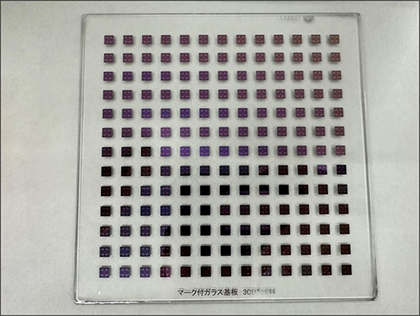
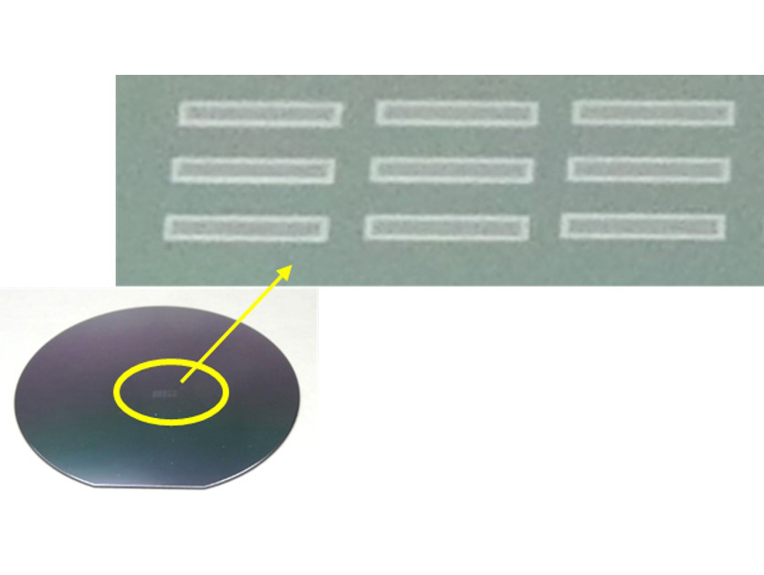
To demonstrate the laser transfer technology developed in the project, we made on a trial basis semiconductor chips having a size of 5 mm x 5 mm and a thickness of 10 µm and successfully transferred them with an accuracy of ±2 µm (3σ) in a demonstration test. The damage to the chips was evaluated by inspecting the transferred chips visually and measuring the transverse rupture strength*3, and no significant damage to the chips in the laser peel transfer process was found. In addition, compound chips having a size of 0.15 mm × 0.70 mm and a thickness of 1 µm or less (such as InP*4 and TFLN*5) were successfully transferred and bonded to silicon substrates, demonstrating the adaptability to the bonding process.
The demonstration has brightened the prospect of solving the issue related to mass-productivity in the bonding process for ultra-thin chips, which has been difficult so far.
3. Future plans
Using the technology, Toray Engineering will further improve and optimize the technology towards the productization of advanced semiconductors. We will continue our efforts towards the implementation of the technology while collaborating with semiconductor manufacturers and related companies and institutions. Through such efforts, we will contribute to the higher performance and lower power consumption of advanced semiconductors, aiming to build a sustainable society.
【Notes】
| *1 | The Project Project name: Research and Development Project of the Enhanced Infrastructures for Post-5G Information and Communication Systems/Development of manufacturing technologies for advanced semiconductors/Development of laser transfer technology for advanced semiconductor bonding Project period: FY2022 to FY2025 Project overview: Research and Development Project of the Enhanced Infrastructures for Post-5G Information and Communication Systems https://www.nedo.go.jp/activities/ZZJP_100172.html (in Japanese) |
|---|---|
| *2 | Industry’s highest level According to research conducted by Toray Engineering as of August 2025 |
| *3 | Transverse rupture strength An index of strength of a material when the material is bent to rupture. Used to evaluate strength properties of semiconductor chips. |
| *4 | InP Abbreviation of a compound of indium and phosphorus. A compound semiconductor of a group III element and a group V element. |
| *5 | TFLN Abbreviation of Thin Film Lithium Niobate, a compound of niobium, lithium, and oxygen. |