- HOME
- Products and Services
- Film-Production Equipment
- Laser Patterning
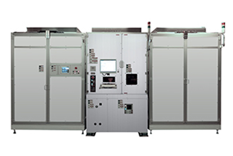
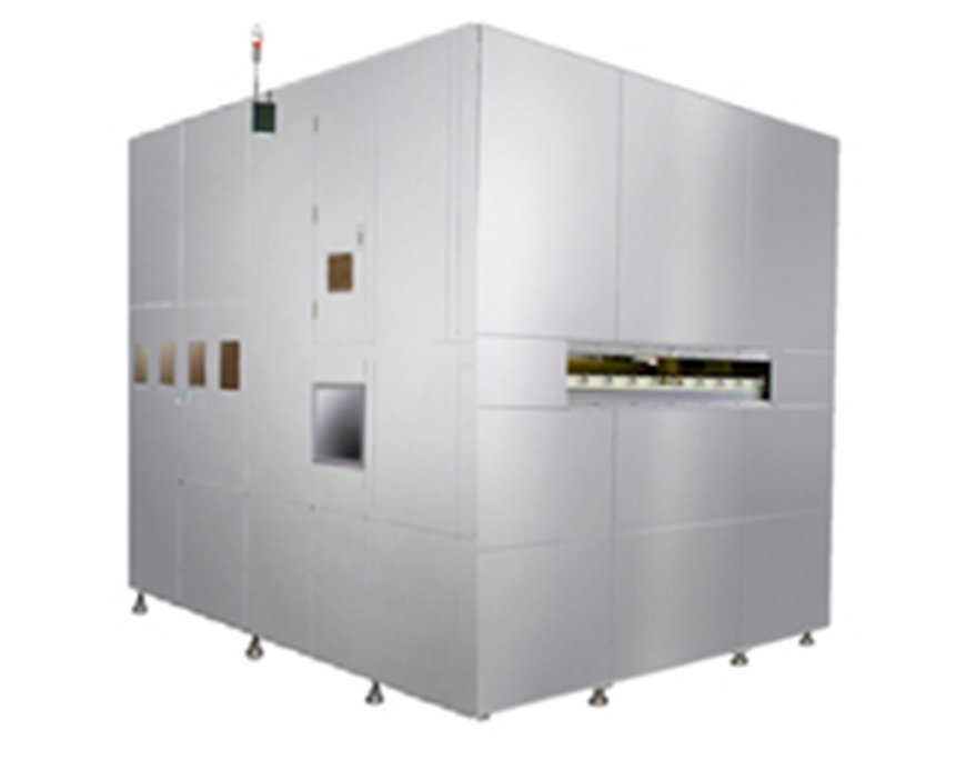
- High Accuracy Laser Patterning Equipment for Thin Metal film
High Accuracy Laser Patterning Equipment for Thin Metal film
Achieving high Accuracy processing onto ultra-large substrates
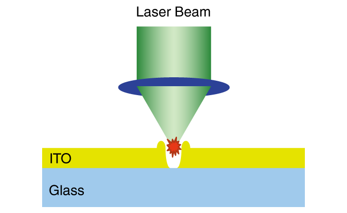
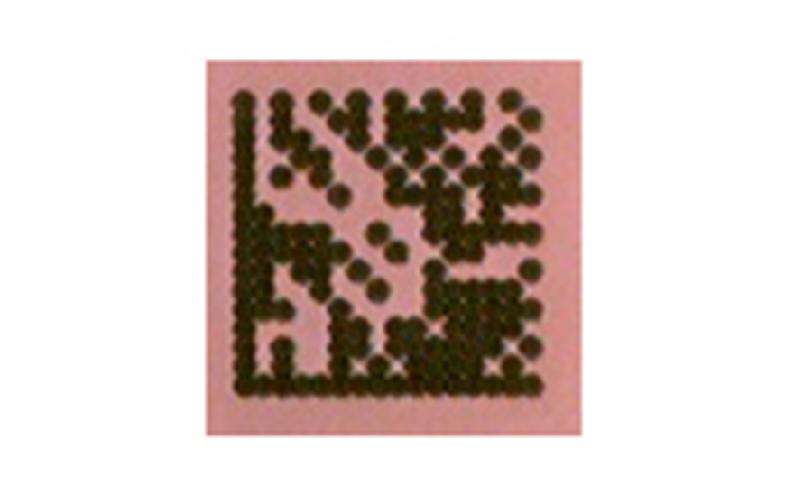
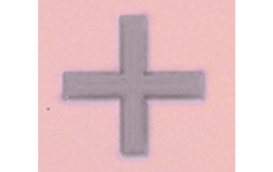
Alignment marks and insulation pattern processing are available for transparent electrode films such as ITO and metal thin films such as Cu and Al.
Achieved high position accuracy processing (± 15 um @ G6) by our unique alignment and patterning technology.
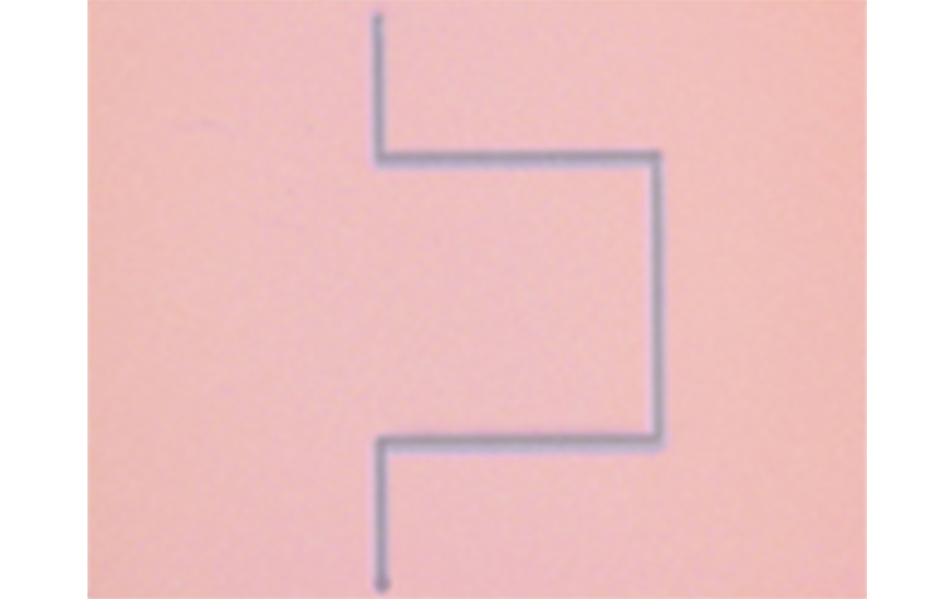
Example
Specification
| Substrate size | ~3370㎜×~2940㎜ *G10.5 generation is available. |
|---|---|
| Laser wavelength | 1064 nm / 532 nm / 355 nm |
| Takt time | Depend patterning specifications. |