- HOME
- Products and Services
- Semiconductor-Production Equipment
- Flip Chip Bonders
- Bonder Series
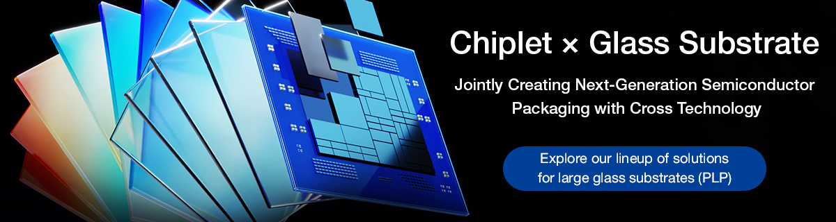
- UC5000 For PLP Bonder
UC5000For PLP Bonder
High-accuracy PLP bonder
Capable of supporting chiplet packaging with a 1 model.
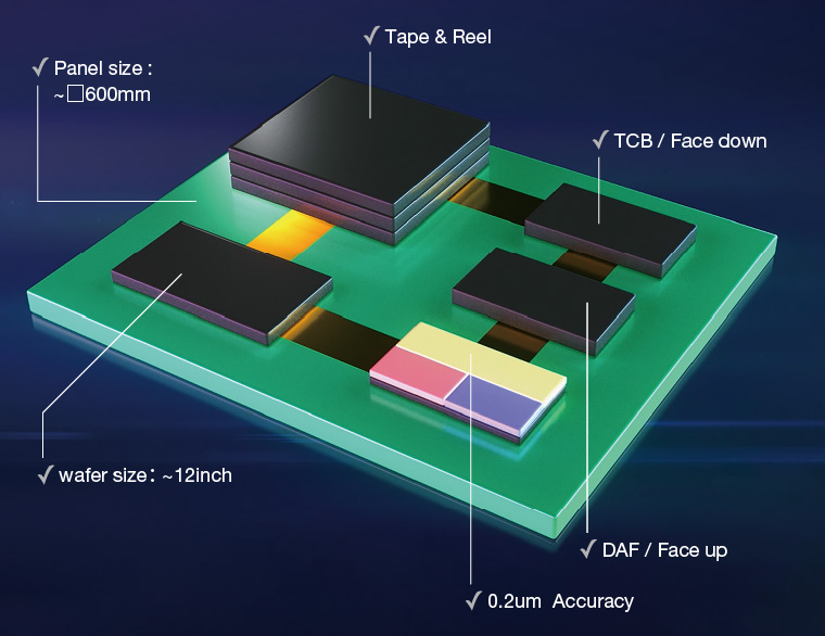
Features
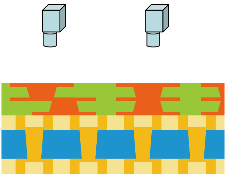
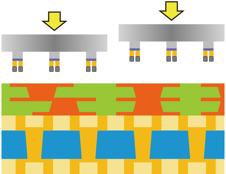
- Supports various bonding process including TCB, DAF, and Hybrid bonding.
- Accommodate 2 wafers or ~600x600mm panel
- Die can be supplied through various methods, wafers, trays, and tape & reel.
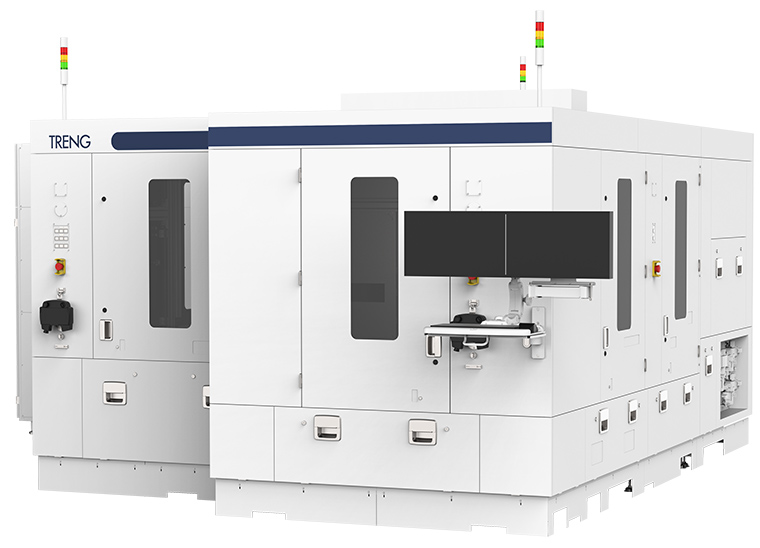
Multi capability
Spec
| Bonding accuracy(3σ) | 0.8 µm (for TCB) 0.2 µm (for Hybrid) |
|---|---|
| Bonding stage | 515 × 510 mm, 600 × 600 mm 300 mm wafer |
| Support die size | ~ 33 × 33 mm |
| Bonding force | 1 ~ 500 N |
| Bonding process | Face down, Face up |
PLP solution
| Cleaning & Inspection | Formulation TGV | Build-up Layer Coating | Drilling | RDL PR & PI Coating / Exposure | Pattern Inspection | Chip Bonding | |
|---|---|---|---|---|---|---|---|
 |
 |
 |
 |
 |
 |
 |
|
| cleaner & HS-Series | Laser & Etching | Coater & VCD | Laser Drill | Coater & VCD | Exposure Deve | INSPECTRA | Bonder |