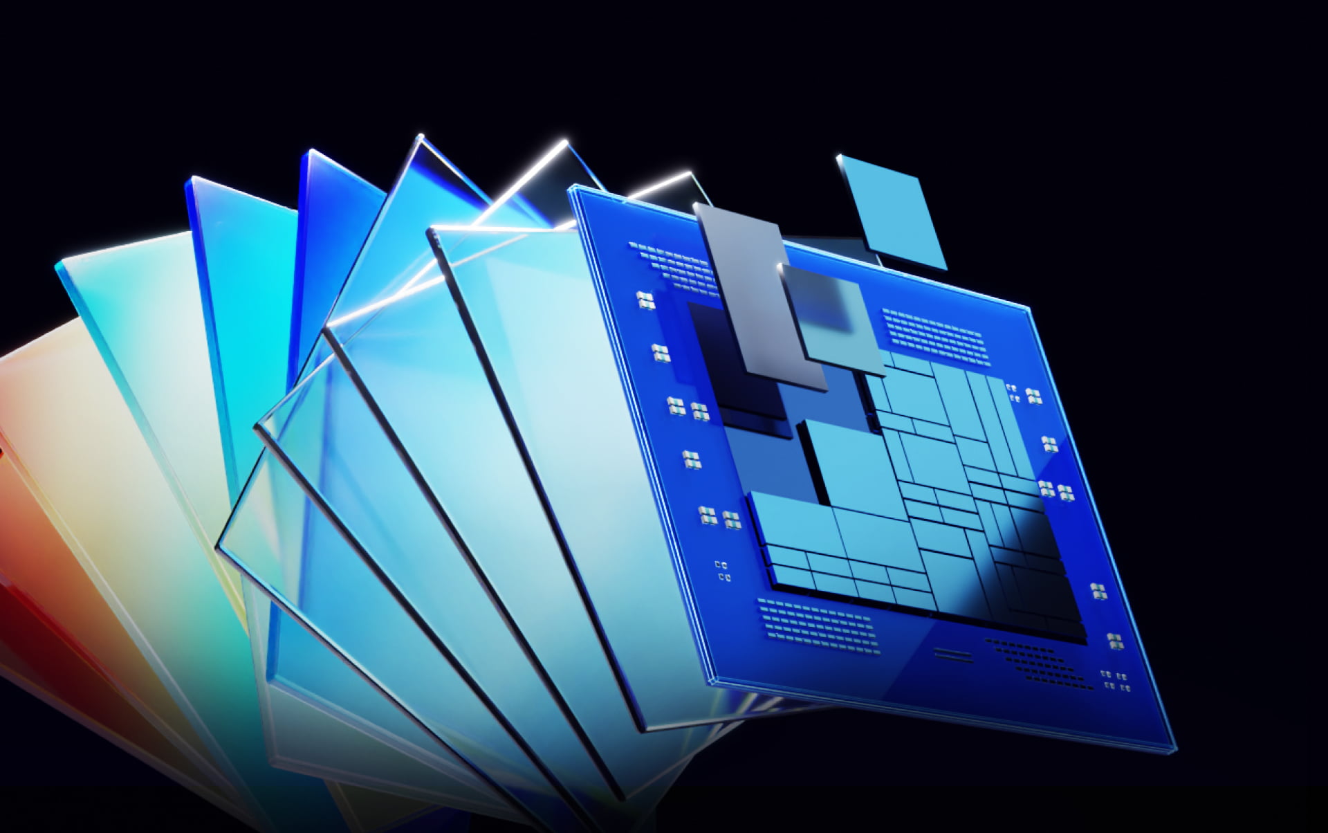
Chiplet×Glass Substrate
Jointly Creating
Next-Generation Semiconductor
Packaging
with Cross Technology
ABOUT
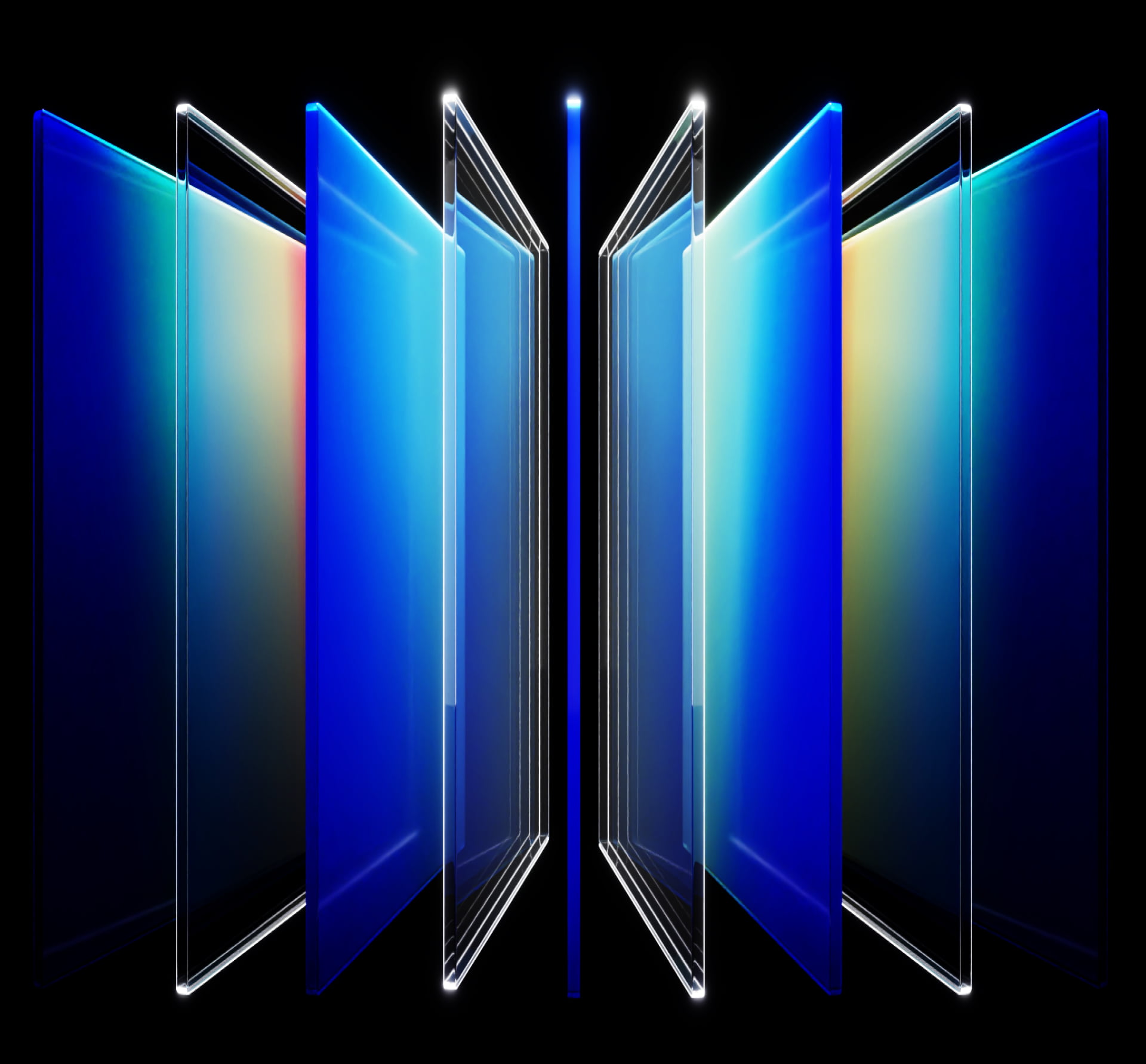
Coating, Inspection, and Bonding
for Large Glass Substrates (PLP)
Providing the core process
for the manufacture of next-generation semiconductor packaging
For more than a quarter of a century since the introduction of the flip chip bonder to the market, Toray Engineering has continued to develop technologies necessary for the manufacture of cutting-edge semiconductor packaging.
Currently, the rapid evolution of generative AI has resulted in a proliferation of hyperscale data centers. In addition to higher performance, increased production capabilities are required of semiconductor packaging.
For this reason, semiconductor manufacturers around the world are beginning to shift to manufacturing with large glass substrates (panel level packaging; PLP), which enable highly efficient manufacturing.
By advancing coating, inspection, and bonding technology cultivated over the years, Toray Engineering has commercialized innovative technologies for glass substrates that increase manufacturing efficiency of advanced semiconductor packaging. Toray Engineering will jointly create next-generation semiconductor packaging with customers by providing high-quality technologies for each process.

and drying equipment

inspection equipment

bonding equipment

used in PLP
PRODUCTS
Providing Japan's leading solutions for
high-end products
Toray Engineering's advanced technical capabilities
enable the manufacture of high-end products
that support cutting-edge technologies and products.
Technologies for Each Process


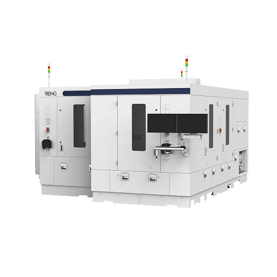
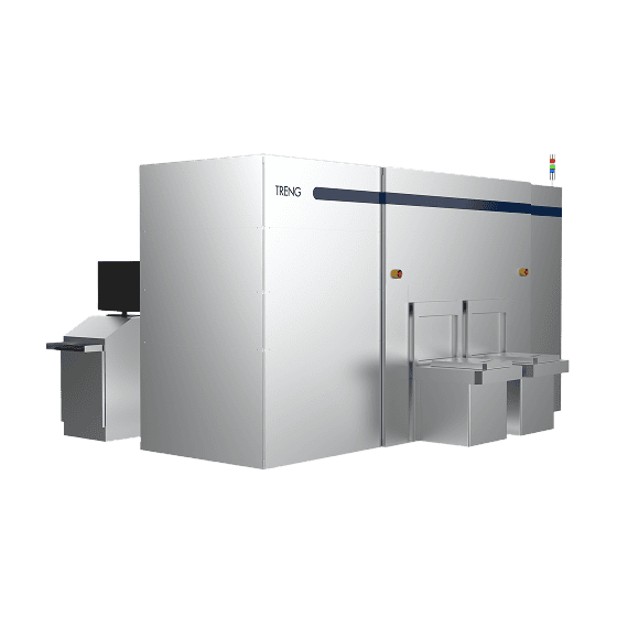
Glass panel inspectionHS-930e
Inspects substrates before and after deposition with high spatial resolution and detects transparent foreign particles.
The combination of optical design and image processing achieves simultaneous inspection of the front and back and high throughput.
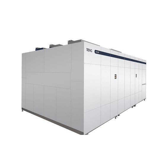
PLP CoaterTC406T-S
To respond to the increasing size of 2.5D packaging, the coating technology cultivated for LCD panels is integrated with the substrate warpage prevention technology used in PLP to achieve high-accuracy, high-density, and high-efficiency rewiring layer formation.
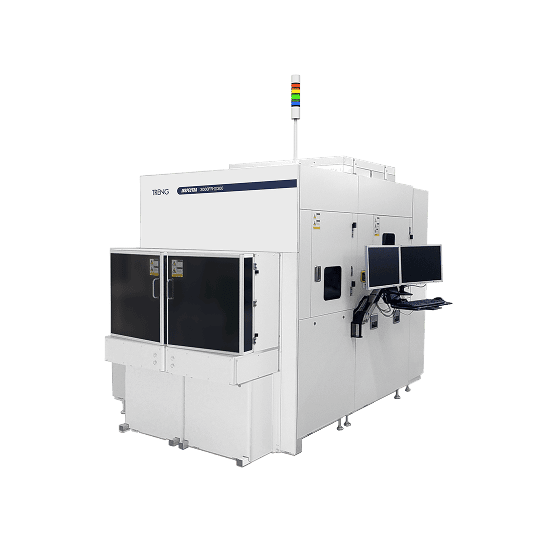
AOIINSPECTRA GR-X
The inspection equipment for large glass substrates is the first in the industry to achieve double-sided inspection and internal defect inspection. The inspection speed is also high, enabling total inspection and contributing to preventing the outflow of defective products.