Wafer Inspection System "INSPECTRA®" Series
![]()
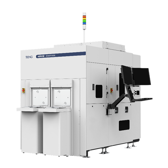
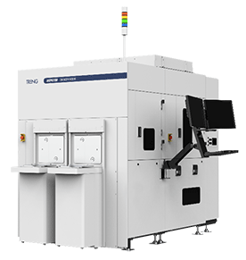
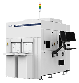
Wafer inspection system "INSPECTRA® SR-Ⅳ"
Wafer inspection system
Overview
Highest speed in the industry
INSPECTRA® Series meet the requests of 100% automatic inspection with high speed and high specifications from front-end to back-end of semiconductor processing.
INSPECTRA® Series are wafer inspection systems with high speed and high sensitivity.
Our original "Die-to-Statistical-Image" comparison method achieves the target defects detection controlling process variation and overkill.
Lineup
SR-IV Series offers improved fast throughput, inspection performance and equipment reliability, usability in addition to the functionality of previous models.
The SR-IV series is twice as fast at high magnification inspection than existing SR-Ⅲ Series.
We meet customer needs with a wide range of lineups, including SR-Ⅳ/SR-Ⅲ Series which achieved high sensitivity and speed inspection, and FR-Ⅲ Series which allowed diced wafer inspection.
Specifications
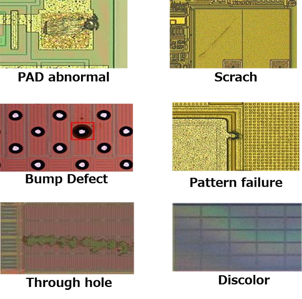
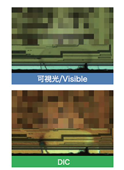
| Defect detection example | Differential interference optical system (DIC) Inner crack detection example |
 INSPECTRA Series |
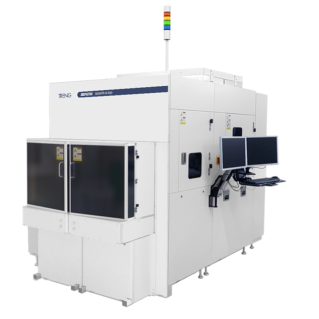
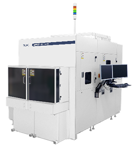
 FR-Ⅲ Series |
Wafer Inspection System "INSPECTRA®" Series lineup
| Model | Feature | Work piece size |
|---|---|---|
| SR-Ⅳ Series | 2x speed up with high magnification inspection than SR-Ⅲ. SR-Ⅳ Series achieved both high sensitivity and high speed 100% inspection to meet the market needs. |
2inch-12inch |
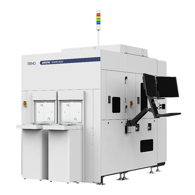
| SR-Ⅲ Series | SR-Ⅲ Series is the successor to SR Series. By process monitoring with 100% inspection, it's possible to prevent missing defects early. |
| Model | Feature | Tape frame size |
|---|---|---|
| FR-Ⅲ Series | Optimal for inspection following dicing or expanding.Automatic tape frame feed. | ≤ 400mm |
| Convenient standard functions | Sensitivity simulation, PAD inspection, Defect color image storage, Non-pattern inspection, Cell to Cell inspection, Die to Die inspection、Automatic defect classification, full image storage, Active auto focus, Ionizer, Recipe sharing, Lighting calibration, Chip rotation/misalignmet correration (FR Series), etc. |
|---|---|
| Extensive range of options | Differential interference optical system, Ring (Dark Field) illumination, Back side/Edge inspection, Result analysis system, Wafer cleaner, Measurement function, Color inspection, AI-ADC (Defect classification by AI), Support for various wafer transport methods (thin/warpage/substrate), Support for vatious communication medhods, etc. |
| Usage track record | LSI, CISs, MEMS, LED, bump/TSV/Via inspection, power semiconductor, SiC, GaN, compound semiconductor |