Wafer internal defect inspection system "INSPECTRA® IR" Series
![]()
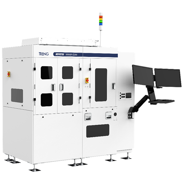
Wafer internal defect inspection system "INSPECTRA® IR" series
Detects defects inside wafers using infrared light
Overview
An infrared internal defect inspection system has been added to the INSPECTRA® series.It is now possible to inspection with both infrared and visual light in one system.
Features
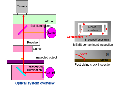
- Uses a high-sensitivity camera and newly developed optical system, supporting both infrared and visible light, to rapidly detect internal defects in wafers
- Uses tried and proved quality product learning algorithm to detect minute defects with a high degree of sensitivity
- Inspection can be performed using both infrared and visible light(Switchable). Meets a wide range of inspection needs
Application examples
- Defect inspection in Si capped structure MEMS wafers
- Internal defect inspection in Image Senser
- Void inspection in bonded wafers
- Defect inspection in high aspect ratio trenches
- Backside crack inspection in High-density wafer
Specifications (IR)
| Pixel resolution | ≥1um |
|---|---|
| Inspection Time | 14 minutes (8 inch wafer,10x faster) |
| Support Wafer Size | 12 & 8 inch and 8inch-2inch |