Luminescence Defect Inspection System "INSPECTRA® PL" Series for Power devices (GaN, SiC)
![]()
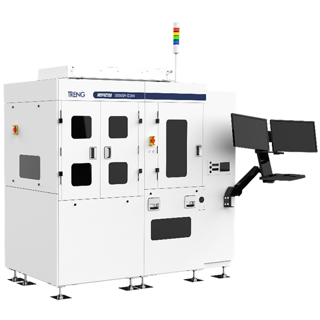
Luminescence Defect Inspection System "INSPECTRA® PL" Series
Photoluminescence (PL) is used to automatically inspect for crystal defects, cracks, and luminescence defects which cannot be detected with visible light surface inspection
Overview
This system uses luminescent images created using photoluminescence (PL) to perform high-speed, high-sensitivity automatic inspection for crystal defects, cracks, and luminescence defects which cannot be detected with conventional visible light surface inspection.
Features
- Unique optical system and inspection algorithm are used for high-speed, high-sensitivity crystal defect detection and categorization.
- Can be mounted as an optional peripheral to a wafer inspection system to not only perform crystal defect inspection during EPI processes, but to carry out integrated prototype and mass production inspection that covers everything up to pattern process surface inspection.
- Visible light inspection and PL inspection can be combined to contribute to greater yield by identifying killer defects.
Specifications
| GaN |   |
 |
|
| SiC | 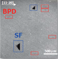 |
 |
|
  |
 |
 |
SiC use (power devices)
| Inspection Sample | SiC wafers, chips |
|---|---|
| Pixel resolution | ≥0.325um |
| Inspection Time | 15 minutes (4 inch wafer, 5x, PL inspection) |
| Suport Wafer Size | 2inch–8inch |
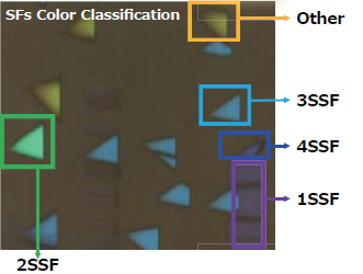
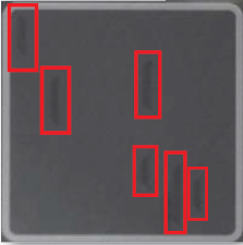
| Target | Crystal defect (BPD, SF), pattern faulure, etc. |
GaN use (power devices)
| Inspection Sample | GaN/sapphire, GaN/SiC, GaN/Si, GaN/GaN wafers and chips |
|---|---|
| Pixel resolution | ≥0.325um |
| Inspection Time | 15 minutes (4 inch wafer, 5x, PL inspection) |
| Suport wafer sizes | 2inch–8inch |
| Target | Crystal defect, crack, pattern failure, etc. |