Luminescence Defect Inspection System "INSPECTRA® PL" Series for Mini・Micro LED
![]()
Luminescence Defect Inspection System "INSPECTRA® PL" Series
Photoluminescence (PL) is used to automatically inspect for crystal defects, cracks, and luminescence defects which cannot be detected with visible light surface inspection
Overview
This system uses luminescent images created using photoluminescence (PL) to perform high-speed, high-sensitivity automatic inspection for crystal defects, cracks, and luminescence defects which cannot be detected with conventional visible light surface inspection.
Features
- Unique optical system and inspection algorithm are used for high-speed, high-sensitivity crystal defect detection and categorization.
- It's also possible to detect brightness changes and wavelength variations of all chips in a wafer.
- Can be mounted as an optional peripheral to a wafer inspection system to not only perform crystal defect inspection during EPI processes, but to carry out integrated prototype and mass production inspection that covers everything up to pattern process surface inspection.
- Visible light inspection and PL inspection can be combined to contribute to greater yield by identifying killer defects.
Specifications
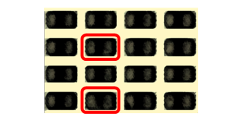
Visual inspection (AOI)
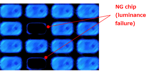
PL inspection
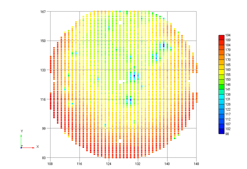
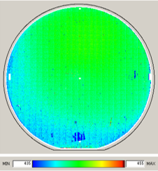
Brightness average map (PL)
Wavelength estimation
| Inspection Sample | LEDWafer, Chip, Substrate |
|---|---|
| Pixel resolution | ≥0.325um |
| Inspection Time | 10mintes(4inch wafer, 10x, PL inspection) |
| Sample size | 2inch–G2.5 |
| Inspection function | PL inspection / Visual inspection (AOI) |
| Target | Luminance failure, shift of emission wavelength, EPI defect, Crack, Pattern failure, etc. |
| Option | Wavelength estimation function Measurement fucntion (chip shift, chip rotation, chip missing) |