Electron Beam
Semiconductor Wafer
Pattern Verification System
”The Die to Database algorithm” that compares design data with SEM images solves systematic problems quickly on the leading-edge semiconductor device manufacturing.
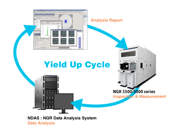
Role of the NGR products on semiconductor manufacturing processes
Semiconductor devices are manufactured by repeated processes of thin film deposition, circuit pattern lithography, etching and impurity atom implantation on silicon wafers. Pattern miniaturization has progressed and minimum pattern width has reached beyond 2 nm on the leading-edge semiconductor devices.
Miniaturization of semiconductor devices contributes to profit for semiconductor manufacturers, however it causes profit loss due to the decrease of the yield rate derived from defects such as pattern short, pattern open during the production process. On semiconductor device business, it is important to inspect and measure these pattern defects and pattern dimensions during the process, improve the manufacturing process and the yield.
The NGR’s geometry verification system is based on Die to Database algorithm and contributes to high sensitivity defect inspection for pattern defects and 2 dimensional mass CD measurement by using the wide FOV electron microscope.
Wafer Geometry Verification System NGR5000 Series
NGR5000 Series contiributes to improve the efficiency of manufacturing processes at manufacturers of NAND memory semiconductors, which are becoming increasingly multilayered to achieve higher performance, and DRAM memory and logic semiconductors, which are becoming increasingly miniaturized.
Wafer Geometry Verification System NGR3500 Series
NGR3520 is the product that improves resolution on electron optics, miniaturizes the minimum inspection pixel size to 1nm and is applicable to the leading-edge device inspection and metrology for beyond 20 nm design rule.