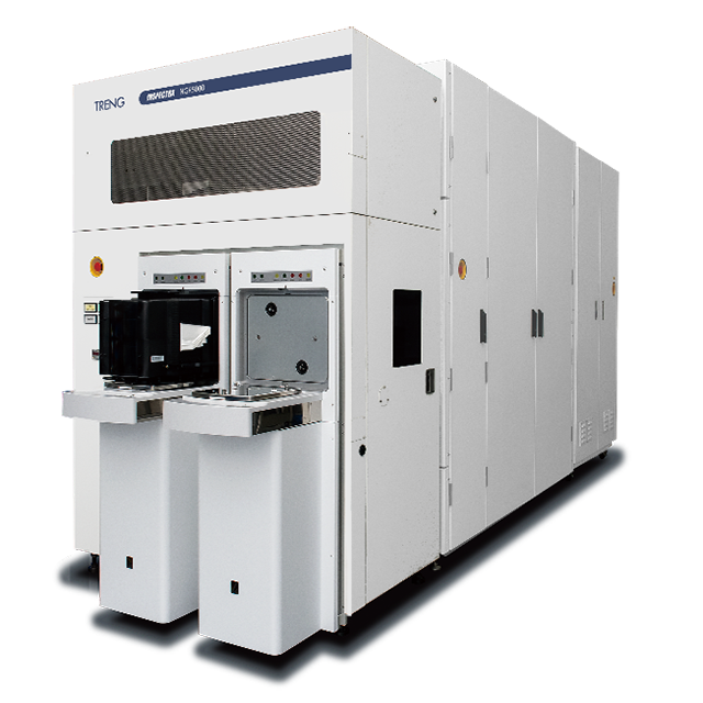
Wafer Geometry Verification System NGR3500 Series

Overview
As the semiconductor device is getting higher performance and more multifunctionality, the combination of a large variety of inspection and measurement is necessary for the process monitoring.
NGR3500 series with wide FOV electron microscope is based on Die to Database algorithm and contributes the drastic yield improvement by high sensitivity defect inspection and 2-dimensional mass CD measurement with high throughput.
<Wafer Geometry Verification System NGR3500 Series Specifications>
| Model | Features | Specification |
|---|---|---|
| NGR3520 | NGR3520 is the product that improves resolution on electron optics, miniaturizes the minimum inspection pixel size to 1nm and is applicable to the leading-edge device inspection and metrology for beyond 10 nm process. | Wafer size:Φ300mm(SEMI compliant V notch wafer) |
| NGR3550 | NGR3550 is the product that is applicable to the wide application beyond 7nm process by wider range of electron beam condition. Besides, new scanning system provides high throughput by enlarging FOV size. | Wafer size:Φ300mm(SEMI compliant V notch wafer) |
| NDAS (NGR Data Analysis System) |
NDAS is the data analysis system with the unique algorithm for statistical analysis. NDAS visualize the valuable data which contributes the yield improvement by importing a large quantity of data outputted by NGR3500 series and analyses them statistically. | Maximum 5 users can access one NDAS server at the same time |
| Application(Actual example) | Hot Spot extraction/Monitoring Process window qualification OPC optimization CD Uniformity measurement CD distribution analysis In-Chip Overlay measurement EPE measurement |
|---|---|
| Option | Dry pump Magnetic field canceller Anti-vibration table NDAS license Pattern classification function Pattern search function Factory automation |
Inquiries
- CONTACT US
-
Japan: Head Office
+81-45-507-3330


