Wafer Geometry Verification System NGR5000 Series
![]()
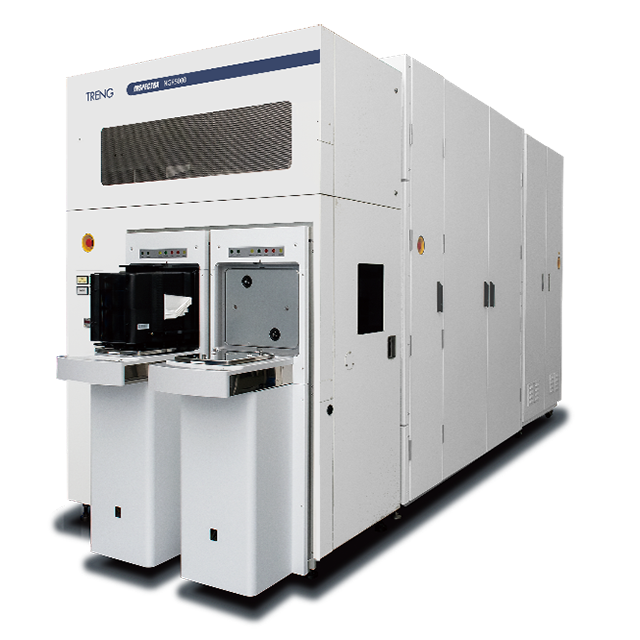
Overview
NGR5000 Series contiributes to improve the efficiency of manufacturing processes at manufacturers of NAND memory semiconductors, which are becoming increasingly multilayered to achieve higher performance, and DRAM memory and logic semiconductors, which are becoming increasingly miniaturized.
NGR5500 has succeeded in increasing the acceleration voltage of electrons used in electron microscopy to 50kV. By increasing the acceleration voltage, it is possible to obtain high quality images of semiconductor devices, which are becoming higher and higher, and to achieve highly accurate inspection and measurement.
NGR5300 is the successor to the existing NGR3500 series. Newly developed optics, image acquisition system, and high-speed stage achieves the inspection/measurement accuracy and throughput required for the advanced semiconductors process.
<Wafer Geometry Verification System NGR5000 Series Specifications>
| Model | Features | Specification |
|---|---|---|
| NGR5500 | NGR5500 uses a variable voltage electron beam to acquire images of a wide field of view. The wide field of view enables inspection and mass CD measurement for the wide-area patterns. Highghly accelerated electron beam is irradiated onto a pattern on a semiconductor wafer, and an image is generated from secondary electron signals and reflected electron signals. For high-aspect patterns, the system can measure the pattern shape, including dimensions and tilt. For multi-layered patterns, overlay measurement of the pattern between layers can be performed. |
Wafer size:Φ300mm(SEMI compliant V notch wafer)) |
| NGR5300 | NGR5300 is the e-beam wafer pattern verification system which is applied to the most advanced semiconductor device. NGR5300 has unique e-beam optics which has wide field of view and has D2DB (Die to Database) algorithm to inspect and measure the pattern on the wafer. NGR5300 is the successor model of NGR3500 series. NGR5300 adopts the latest technologies on XY stage, E-beam optics, platform, and processing system to achieve higher throughput and higher precision on inspection and measurement. |
Wafer size:Φ300mm(SEMI compliant V notch wafer) |
| NDAS (NGR Data Analysis System) |
NDAS is the data analysis system with the unique algorithm for statistical analysis. NDAS visualize the valuable data which contributes the yield improvement by importing a large quantity of data outputted by NGR3500 series and analyses them statistically. | Maximum 5 users can access one NDAS server at the same time |
| Application(Actual example) | Hot Spot extraction/Monitoring Process window qualification OPC optimization CD Uniformity measurement CD distribution analysis In-Chip Overlay measurement EPE measurement |
|---|