Overlay measurement system "OM-7000H"
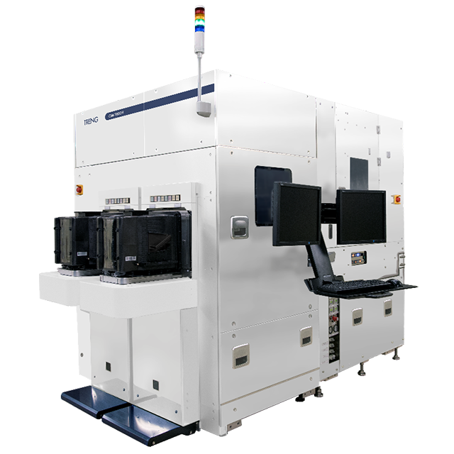
OM-7000H
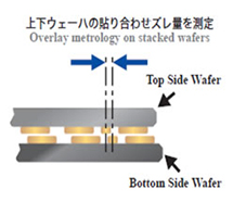
Measures wafer bonding misalignment and top-to-bottom alignment with a high degree of precision
Overview
Measures wafer bonding misalignment and top-to-bottom alignment to a high degree of precision.
Features
- Support for completely automatic measurement
- Supports both transmitted and reflected measurement
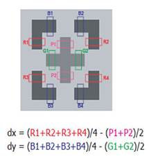
- High-precision measurement using a unique measurement algorithm
- High-precision focus using PZT stage
- Automatic defect image storage
- Can also measure top-to-bottom overlay patterns
- Can be installed in a wafer bonding equipment
Specifications (OM-7000H)
Application examples: Stacked image sensors, stacked memory (Flash, D-RAM), next-generation IGBT, etc.
| Measuring Method | Edge detection by IR |
|---|---|
| Sample | φ300mm Stacked Wafers |
| Lighting | Reflected IR / Transmitted IR |
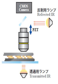
| Objective lenses | 5x: Global alignment 20x: Measurement |
|---|---|
| Repeatability | 3σ≦10nm |
| Measurement Time | 5sec/point |
|---|---|
| Clean class | Class 1 |
| Full Automation | GEM300 compliant |