- HOME
- Products and Services
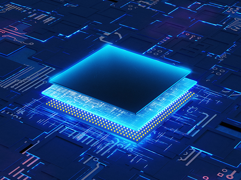
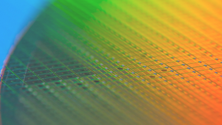
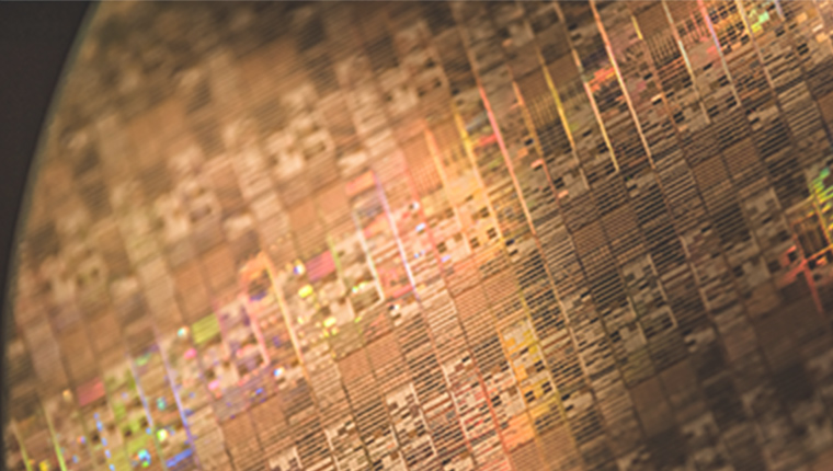
- Semiconductor-Production Equipment
Semiconductor-Production Equipment
Product Categories
Foreign particle inspection system for Panel Level Package (PLP)
Inspection equipment employing Toray Engineering’s unique optical technology has earned high reliability in the inspection of glass substrates, which require high precision.

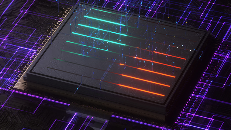
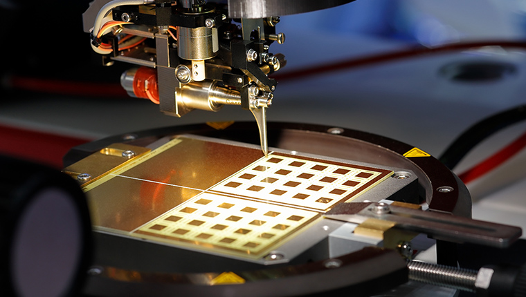
Coating Equipment for advanced semiconductor package
Building on our expertise in high-precision coating and large glass handling technologies developed through display manufacturing, we are contributing to advanced semiconductor production.
Bonding Equipment
Bonder series contributing to advanced semiconductor package manufacturing.
We can meet a wide range of needs, from R&D to mass production.
Our lineup has a variety of bonders for 3D bonding with TSV, FOWLP, FOPLP, optical devices, and other purposes.

Laser Micro Trimming Equipment
By laser irradiation, this equipment performs failure Mini LED removal, semiconductor memory repair, and resistance fuse trimming.
Optical Semiconductor inspection equipment
We have a full line-up of inspection systems for the semiconductor production process. All of these systems have earned an outstanding reputation on the production line for their high reliability, ease of operation and minimal running cost.
Electron Beam Semiconductor Wafer Pattern Verification System
”The Die to Database algorithm” that compares design data with SEM images solves systematic problems quickly on the leading-edge semiconductor device manufacturing.